Features
•Supply Voltage Range = 3.0 Vdc to 18 Vdc
•Capable of Driving Two Low−Power TTL Loads or One Low−Power Schottky TTL Load Over the Rated Temperature Range
•Triple Diode Protection on All Inputs
•Pin−for−Pin Replacement for CD4069UB
•Meets JEDEC UB Specifications
•NLV Prefix for Automotive and Other Applications Requiring Unique Site and Control Change Requirements; AEC−Q100 Qualified and PPAP Capable
•These Devices are Pb−Free and are RoHS Compliant

Security policy

Delivery policy

Return policy
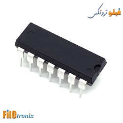
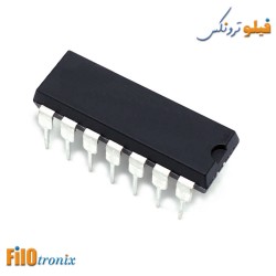
The MC14069UB hex inverter is constructed with MOS P−channel and N−channel enhancement mode devices in a single monolithic structure. These inverters find primary use where low power dissipation and/or high noise immunity is desired. Each of the six inverters is a single stage to minimize propagation delays.
You might also like
Features
•Supply Voltage Range = 3.0 Vdc to 18 Vdc
•Capable of Driving Two Low−Power TTL Loads or One Low−Power Schottky TTL Load Over the Rated Temperature Range
•Triple Diode Protection on All Inputs
•Pin−for−Pin Replacement for CD4069UB
•Meets JEDEC UB Specifications
•NLV Prefix for Automotive and Other Applications Requiring Unique Site and Control Change Requirements; AEC−Q100 Qualified and PPAP Capable
•These Devices are Pb−Free and are RoHS Compliant